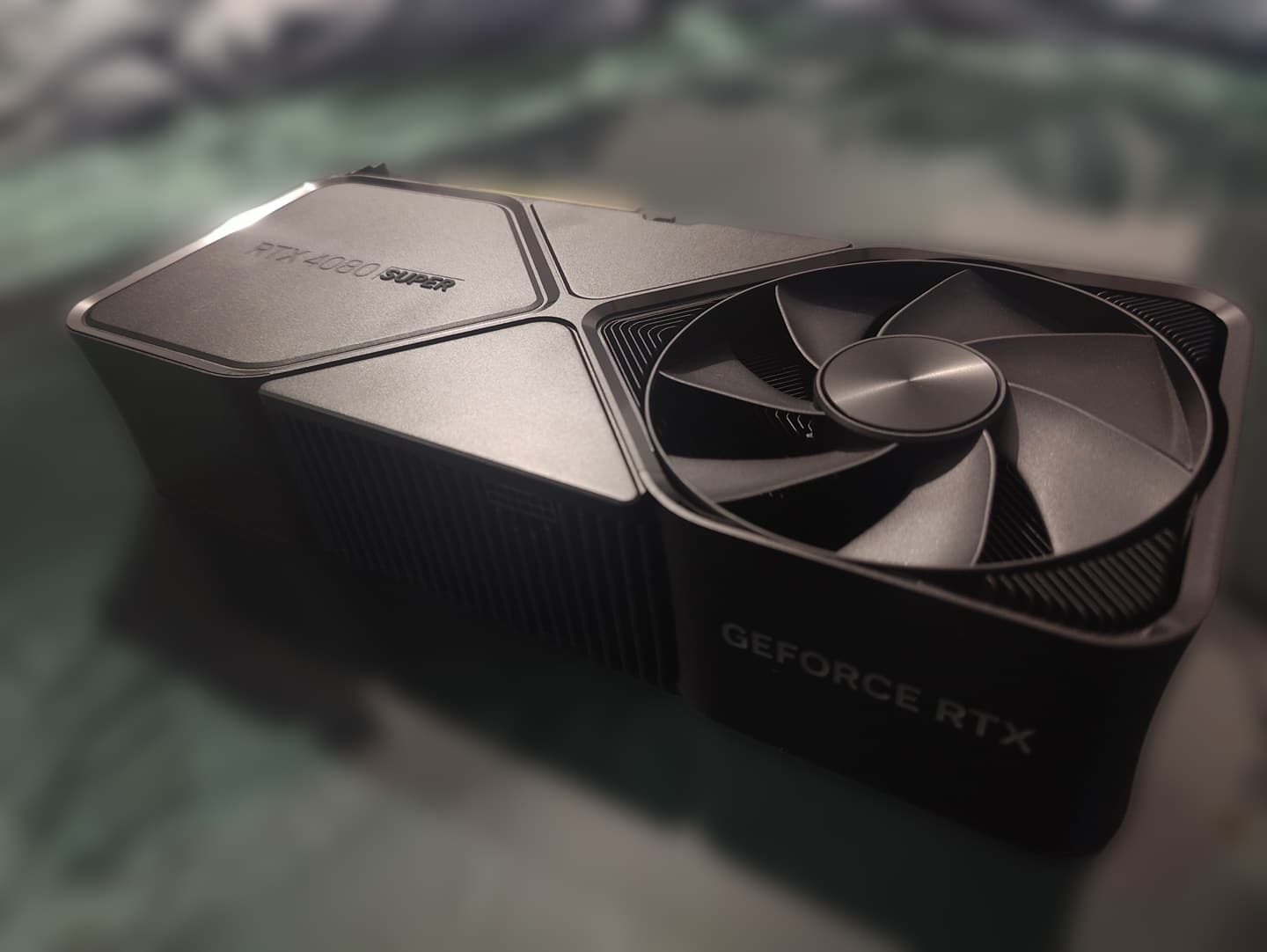
The latest rumors from Chiphell claim that the NVIDIA GeForce RTX 5090 will feature a 448-bit bus, up from 384-bit on the RTX 4090. This follows previous reports claiming that the Blackwell flagship would leverage a 384-bit or the full-fledged 512-bit bus available on the GB202 die. When paired with 28 Gbps of GDDR7 graphics memory, this would produce an external bandwidth of 1568 GB/s.
A 448-bit memory bus implies the use of 14x 32-bit memory controllers, each connected to a 2 GB memory chip. This gives us an overall 28 GB VRAM buffer, 4 GB higher than the RTX 4090 and 3090. For reference, the GeForce RTX 4090 has a peak bandwidth of 1008 GB/s, indicating a 56% uplift for the RTX 5090.
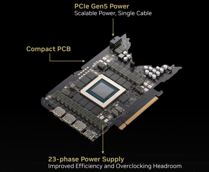
According to @kopite7kimi, NVIDIA will use a triple-part PCB for the RTX 5090, consisting of the Main Board, IO Rigid Board, and the PCIe-slot component. A multi-part board would give the heatsink designers enough room to build a slimmer (and effective) cooling solution. After all, the RTX 4090 and 4080 have grown excessively thick.

The GeForce RTX 5090 will leverage the GB202 GPU featuring 12 GPCs, each comprising 8 TPCs and 14 SMs. This adds up to a maximum shader count of 24576, up from 18432 on the AD102. Like the RTX 4090, the Blackwell flagship will feature a cut-down GB202 die with anywhere between 18000 to 24000 FP32 cores and the corresponding SM and TPCs.
The GB202 GPU powering the GeForce RTX 5090 will feature an on-die partition (hints at it) that divides the shader cluster into two parts, thereby laying the groundwork for future modular/chiplet products. We’ll likely see a high-speed crossbar connecting the two segments featuring their respective L2 cache and memory controllers.
-
 Intel i9-14900K/13900K CPUs Unstable even with Baseline Power Profile: Crashes in Games Persist
-
 AMD Ryzen 7 8840U/7840U is ~2x Faster than the Snapdragon X Elite in Gaming (At the Same Power)
-
 AMD Ryzen AI 300 “Strix Point” Uses Cut-Down CPU Cores & Similar Instruction Throughput as Zen 4
-
 AMD Ryzen 9000 vs Intel 15th Gen/Core Ultra 300 CPUs Specs, Pricing, and Release Date