In the PC market, DRAM is mainly found in three forms: DDR5, LPDDR5, and GDDR6/GDDR6X, along with their predecessors. DDR5 is used in laptops and desktops, while LPDDR5 is used in smartphones and low-power notebooks. GDDR6/GDDR6X (soon GDDR7) are used in graphics cards for storing the textures and other 3D assets used by modern video games. In this post, we break down the differences between the three different types of DRAM:
- DDR4 was the defacto memory for PCs over the last decade, with data rates of up to 3,200 Mbps.
- DDR5 started with a base transfer rate of 4,800 Mbps but has increased to 6,400 Mbps. Overclocked variants go as high as 7,200 Mbps.
- LPDDR4 (and LPDDR4X) supported data rates of up to 4,267 Mbps and has largely been replaced by LPDDR5 and LPDDR5X.
- LPDDR5 typically offers a data rate of up to 6,400 Mbps, while LPDDR5X should up it to 8,533 Mbps.
- GDDR6 (and GDDR6X) have been the primary graphics memory for nearly a decade. They power gaming GPUs, including the RTX 4090/RX 7900 XTX. With a per-pin bandwidth of 20 Gbps, they are among the fastest in the world.
- GDDR7 increases the per-pin bandwidth to 32 Gbps, with plans for 48 Gbps chips in the future. It also raises the peak memory density from 32Gb to 64Gb.

LPDDR5 is one of the most power-efficient memory standards. Thanks to Dynamic Voltage Scaling (DVS), LPDDR5 supports two voltage modes: 1.05V (C) and 0.5V (I/O) while operating at higher frequencies and 0.9V (C) and 0.3V (I/O) when idle. Like LPDDR4/4X, LPDDR5 features 2x 16-bit channels and a burst length of 16 per channel. Burst lengths of 32 are also supported in some configurations.
LPDDR4 and LP4X support two Frequency Set Points (FSPs) for C/A (Command/Address) and DQ while LPDDR5 bumps it up to 3, allowing for rapid switching across the three frequencies at extremely low power. Another power-saving technology, Write X allows the transfer of certain bit patterns to contiguous memory locations without toggling the DQ bits on the channel.

Burst-length: When the CPU or cache requests new data, the address is sent to the memory module and the needed row, then the column is located (if not present, a new row is loaded). Keep in mind that there’s a delay after every step.
After that, the entire column is sent across the memory bus in bursts. For DDR4, each burst was 8 (or 16B). With DDR5, it has been upgrades to 16 (up to 32B). There are two bursts per clock and they happen at the effective data rate. Furthermore, similar to LPDDR4, DDR5 has 2x 32-bit channels per DIMM for a total of four channels in a dual-DIMM configuration. The prefetch and BL have also been increased to 16. This figure is ideal as each cache line in memory is of the same size.
| LPDDR5 | DDR5 | GDDR7 | |
|---|---|---|---|
| Memory Size | 2Gb to 32Gb | 8Gb to 64Gb | 8Gb to 64Gb |
| Burst Length | 16 | 16 | 16 |
| Prefetch | 16n | 16n | 32n |
| Banks | 16 | 32 | 16 |
| Speed | Up to 6400 Mbps | Up to 8400 Mbps | Up to 48 Gbps (per pin) |
| Voltage | 1.05V/0.9V core 0.5V/0.3 V I/O | 1.1V VDD 1.8V VPP | 1.2V VDD/VDDQ 1.8V VPP |
DDR5 features 2x 32-bit channels per DIMM (DDR4 had one 64-bit per channel), with a burst length of 16 and a prefetch of 16n per channel (DDR4 had half as much). DDR5 and LPDDR5 support speeds of up to 6,400 Mbps per the JEDEC standard. We’re already seeing overclocked DDR5 modules hit 7,200 Mbps and higher, something LPDDR5X should also achieve.
LPDDR5 supports memory densities of up to 32Gb per channel, while DDR5 can go as high as 64Gb. Both support the same 16n prefetch and a 16-beat burst length per transaction.

DDR5 has a complex memory bank structure with 32 banks per channel. These are divided into eight bank groups of four banks each. LPDDR5 has a more flexible bank architecture. It supports three bank modes: four banks with four bank groups (bank group mode), eight banks, and sixteen banks.
The bank group mode allows transfer rates higher than 3,200Mbps alongside burst lengths of 16 or 32. The eight-bank mode allows all transfer rates with a burst length of 32, while the sixteen-bank mode is for bandwidths under 3,200Mbps with a burst length of 16 or 32.

GDDR7 picks up after GDDR6, doubling memory bandwidth and chip density. It shifts from NRZ (PAM-2) to PAM-3 signaling, thereby increasing the bandwidth by 50% per transfer. The per pin bandwidth has been boosted to 48 Gbps, though most 1st generation variants will be limited to 32 Gbps. This improves the peak bandwidth of a GPU with a 384-bit bus to 1536GB/s for the first wave of devices.
| GDDR7 | GDDR6X | GDDR6 | |
|---|---|---|---|
| Bandwidth (per pin) | up to 48 Gbps | up to 24 Gbps | up to 24 Gbps |
| Max Chip Density | 8 GB (64 Gb) | 4 GB (32 Gb) | 4 GB (32 Gb) |
| Bandwidth (384-bit) | 1536 GB/s | 1125 GB/sec | 1125 GB/sec |
| DRAM Voltage | 1.2 V | 1.35 V | 1.35 V |
| Data Rate | QDR | QDR | QDR |
| Signaling | PAM-3 | PAM-4 | NRZ (PAM-2) |
| Burst Rate (per ch.) | 16 | 16 | 16 |
| Prefetch (per ch.) | 32n | 16n | 16n |
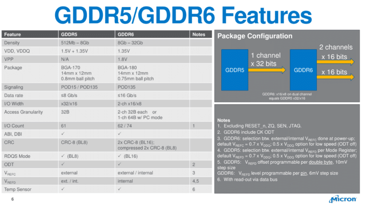
GDDR7 memory features a 32-bit channel per chip sub-divided into four 8-bit channels. In comparison, GDDR6 has two 16-bit channels which can also act as a single 32-bit channel. The burst rate is unchanged at 16 beats per channel, but the prefech has been doubled from 16n to 32n. This effectively doubles the amount of data prefetched per cycle.
Like its predecessor, each GDDR7 memory channel consists of 16 memory banks. This raises the peak chip density to 64 Gb (8GB), though the initial products will retain the 32 Gb (4GB) upper limit of GDDR6. Eventually, you can expect memory capacities of up to 192GB using a 384-bit for the workstation and data center markets.

For power efficiency, GDDR7 reduces its voltage from 1.35 V to 1.2 V. Similar to DDR5, it also includes on-die ECC. Much like DDR5, this error correction will be limited to data in the memory cells. Its primary goal will be to ensure data integrity within a cell or row during refreshes. Like standard ECC, data corruption while transferring to another device won’t be detected.


