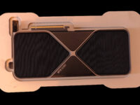
Following AMD’s decision to withdraw from the high-end graphics card market (with RDNA 4), NVIDIA has decided to take things lightly. Or so the rumors go. As per @XpeaGPU, the top-end GeForce RTX 5090/5090 Ti GPU will leverage a monolithic die rather than the previously rumored chiplet design. NVIDIA was planning to release a monstrous modular gaming GPU with HBM memory. The HBM3E memory was going to come from Micron, offering ample bandwidth and efficiency for a gaming-centric chip.
Of course, the said chip would have likely cost as much as the infamous Titan Z “Multi-GPU” graphics card ($3000, in case you don’t remember). The use of a monolithic design means that the GeForce RTX 5090 will offer the same kind of generational gains as its predecessors, somewhere between 60% and 80%.
The B100 Tensor Core Accelerator will still be a chiplet design with multiple compute dies and 3D stacked HBM3E memory. Synchronizing data center workloads between disaggregated dies is much easier than gaming, as latency isn’t that big of an issue (or is easier to hide).
Both the RTX 5090 (Gaming) and the GH100 (Data Center) are expected to leverage TSMC’s 3nm (N3) node. Like AMD’s chiplet designs, NVIDIA’s first modular GPU will be built using TSMC’s CoWoS packaging technology. An early-to-mid 2024 release is expected for the “H100” Data Center GPU, followed by the RTX 5090 and Co. later that year.


