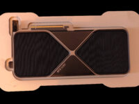
NVIDIA will launch its next-gen Blackwell graphics architecture in the second half of 2024, strengthening its grip over the AI and gaming GPU markets. The B100 Tensor core accelerator/GPU will launch first, followed by the GB200 “Grace Blackwell” Superchip combo. NVIDIA’s AI-centric conference GTC 2024 is scheduled to be held from the 17th to the 21st of March, and that’s where we expect the Blackwell architecture to debut.

Dell SVP Robert L. Williams accidentally divulged the wattage of the B200 during an investor briefing. According to Williams, the B200 will have a power budget of 1000W per GPU. The Dell data center team is excitedly looking forward to it, and the performance gains it brings to generative AI. Expressing confidence in his engineers, he believes that direct liquid cooling isn’t needed for 1000W GPUs such as the B200.
Dell Hopes to Tame NVIDIA’s 1000W GB200 Superchips Using Its Engineering Prowess


Dell will likely use liquid-cooled rack solutions, much like the ones used by its rivals Super Micro, Gigabyte, and HPE. These are highly effective and economical, reducing electricity costs and noise by 45-55%.
Obviously, any line of sight to changes that we’re excited about what’s happening with the H200 and its performance improvement. We’re excited about what happens at the B100 and the B200, and we think that’s where there’s actually another opportunity to distinguish engineering confidence. Our characterization in the thermal side, you really don’t need direct liquid cooling to get to the energy density of 1,000 watts per GPU.
That happens next year with the B200. The opportunity for us really to showcase our engineering and how fast we can move and the work that we’ve done as an industry leader to bring our expertise to make liquid cooling perform at scale, whether that’s things in fluid chemistry and performance, our interconnect work, the telemetry we are doing, the power management work we’re doing, it really allows us to be prepared to bring that to the marketplace at scale to take advantage of this incredible computational capacity or intensity or capability that will exist in the marketplace.
Robert L. Williams, Dell SVP

NVIDIA’s Blackwell GPUs are expected to leverage HBM3e memory, with at least six stacks surrounding the core. The GB200 may use a chiplet design with an even more complex memory system, but it’s too soon to tell. While AMD decided to opt for a modular design with its MI300, NVIDIA has continued to push the boundaries of monolithic designs using TSMC’s cutting-edge 5nm node and will likely do so with the 3nm (N3) process as well.


