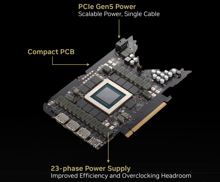
According to the latest rumors, NVIDIA’s next-gen GeForce RTX 5090 will feature a TBP (Total Board Power) of up to 600W. The tip comes from well-reputed tipster @kopite7kimi who claims that the Blackwell gaming flagship will have a peak power rating of 600W. That’s 150W higher than the RTX 4090, the fastest gaming graphics card. Meanwhile, the RTX 5080 will allegedly come with a TBP of 400W, up from 320W on the RTX 4080 and the 4080 Super.

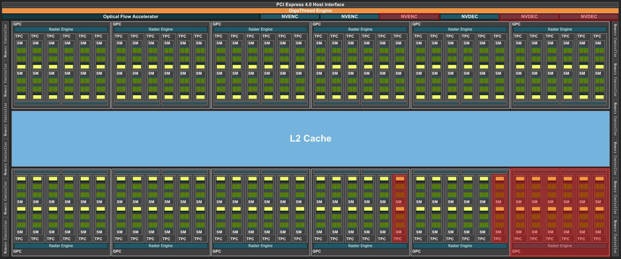
The GeForce RTX 5090 will leverage the GB202 GPU consisting of 12 GPCs (Graphics Processing Clusters), each packing 8 TPCs (Texture Processing Clusters). A TPC includes two SMs (Streaming Multiprocessors) or 256 FP32 cores, implying a total shader count of 24,576 for the GB202.
The GB202 will be paired with 16 GDDR7 memory dies via a 512-bit bus, amounting to 28 GB to 32 GB of graphics memory, depending on the bus width. Depending on the performance targets, NVIDIA can decide to equip the RTX 5090 with a 384-bit, 448-bit, or the whole 512-bit memory bus. When paired with 28 Gbps of GDDR7 graphics memory across a 512-bit bus, we get an external bandwidth of 1568 GB/s.

We expect 17000-20000 FP32 cores (133 to 156 SMs) on the shader side, implying 2 fully or 4 partially disabled GPCs. The L2 cache should scale with the shader and memory bus, coming in at around ~128 MB for the full-fat die.
The GeForce RTX 5080 allegedly features the same shader configuration as the 4080 with 7 GPCs, each featuring 6 TPCs or 12 SMs. This produces an overall core count of 10752, up from 10240 on the AD103 and the RTX 4080 Super. The bus width will remain the same at 256-bit, but the faster GDDR7 memory should result in an external bandwidth of up to 896 GB/s (up from 736 GB/s on the RTX 4080 Super).

According to a report from mydrivers, NVIDIA was forced to redesign the top metal layers and bumps of its GPUs, gaming, and AI. The reason was a mismatch in the coefficient of thermal expansion (CTE) between the GPU die, LSI bridging, RDL interposer, and the main substrate, which can lead to chip warpage and system failure. The updated TBPs accompany the redesign, likely aimed at maximizing the performance targets after a delayed release window.


