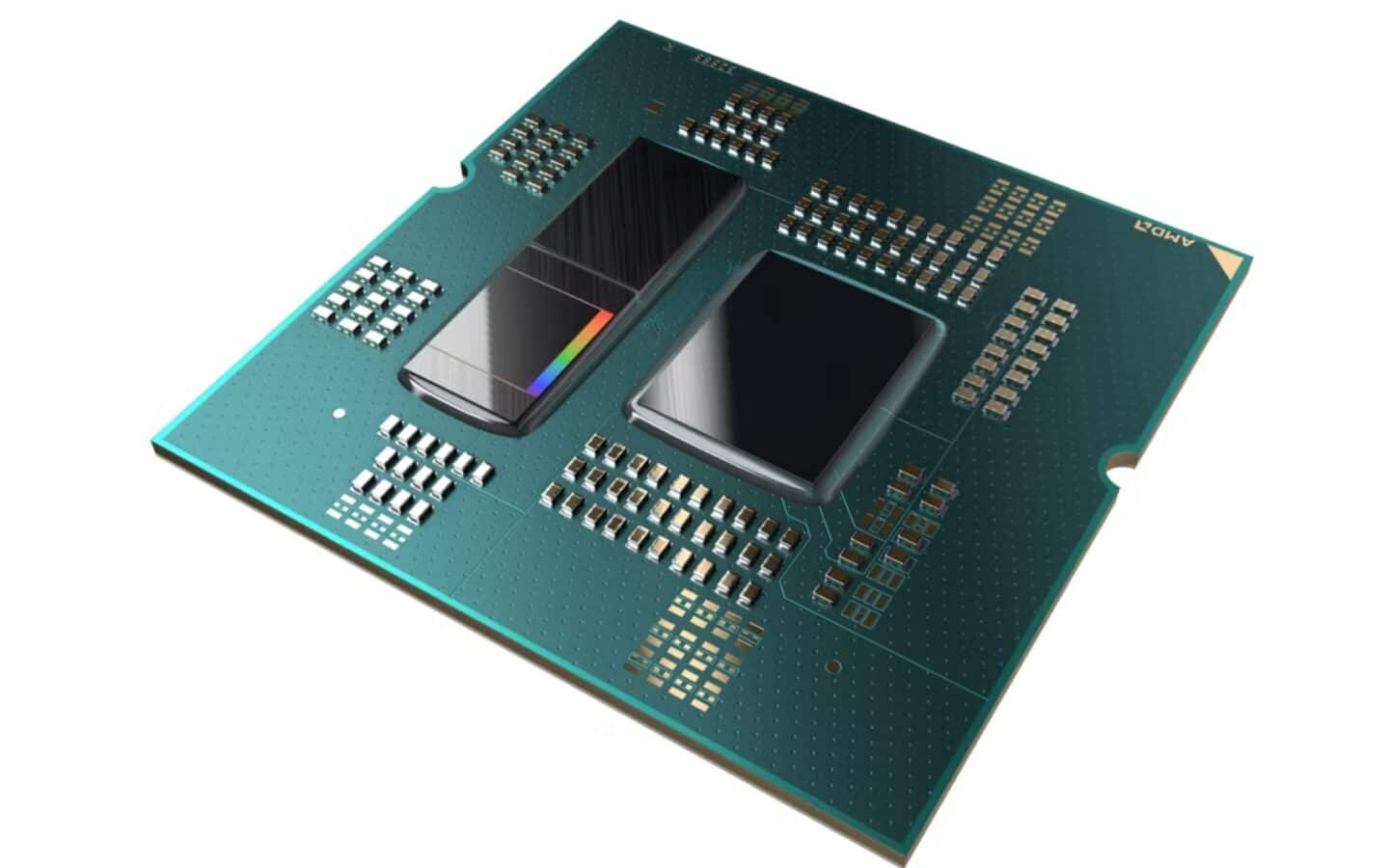
AMD’s Ryzen CPUs are made up of core complexes called CCDs and/or CCXs. But what is a CCX and how is it different from a CCD in an AMD processor? Let’s have a look. There are many factors responsible for AMD’s recent success in the consumer market. But, the chiplet or MCM design (Multi-chip Module) is at the heart of it. It allowed AMD to increase the core counts to never-before-seen figures in the consumer market and set the groundwork for a revolution of sorts.
The Ryzen 9 5950X features 16 cores while the Threadripper flagship, the 3990X boasts an insane core count of 64, the same as the Epyc Rome parts. This means that, at any given price point, AMD can deliver more cores, more threads, and therefore, better multi-threaded performance, than Intel can, even after price cuts.
What is an AMD CCD and CCX
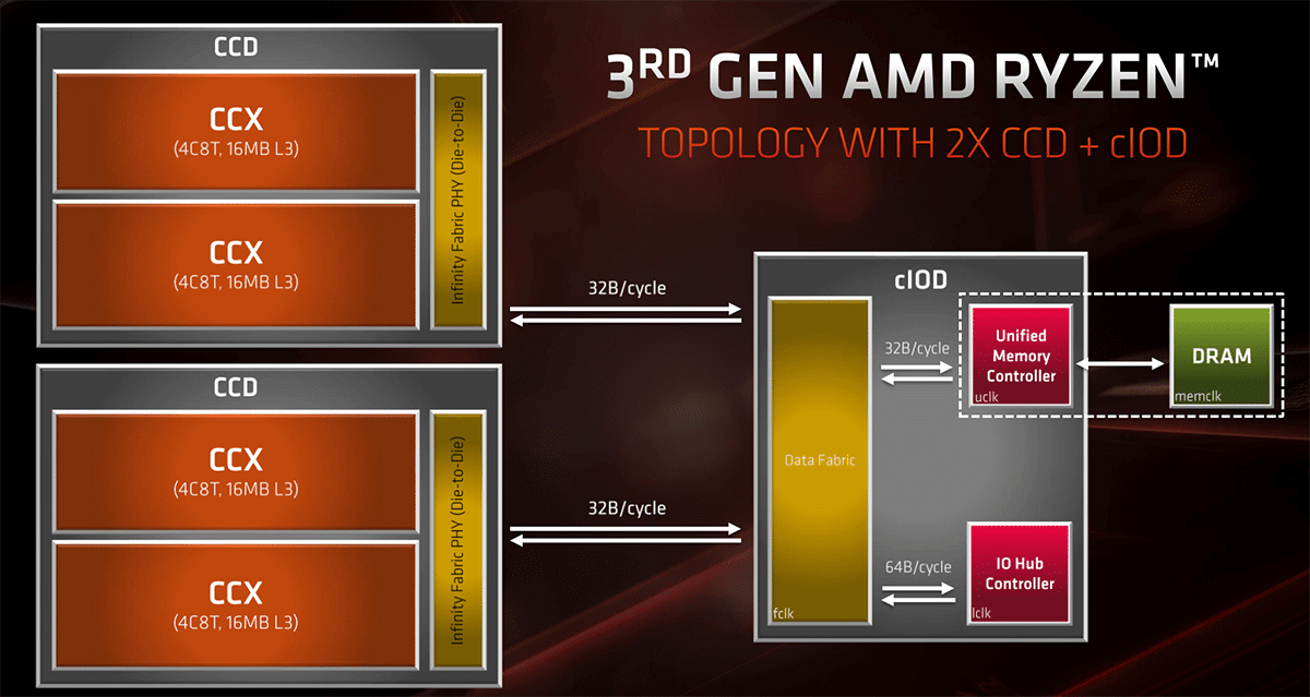
These two functional units lie at the heart of AMD’s modular approach to Ryzen. The basic unit of a Ryzen processor is a CCX or Core Complex, a quad-core/octa-core CPU chiplet with a shared L3 cache. In newer Ryzen 3000 and 5000 parts, the amount of L3 is higher and it’s referred to as “Gamecache.”
The basic unit of a Ryzen processor is a CCX or Core Complex, a quad-core/octa-core CPU model with a shared L3 cache.
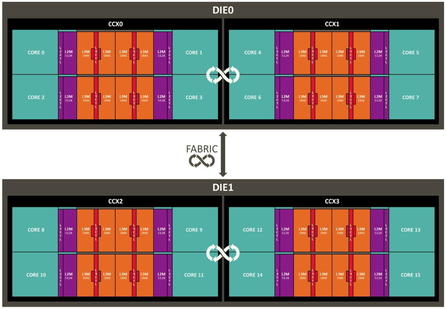
There are pros and cons to having the CCX be Ryzen’s basic functional unit. A negative is that the baseline cost of manufacturing can be somewhat on the high end since AMD needs to pay for a minimum of four cores. However, this is offset by the fact that Team Red salvages partially functional CCXs with, say, two or three functional cores, to create different SKUs. For example, the Ryzen 5 5600X features two CCXs/CCDs, each of which has one core disabled, for a total of 6 functional cores.
However, while CCXs are the basic unit of silicon dabbed, at an architectural level, a CCD or Core Chiplet Die is your lowest level of abstraction. It is the fundamental CPU unit (die) manufactured in high volume for use across all Ryzen/Epyc processors. A CCD consists of one or two CCXs paired together using the Infinity Fabric Interconnect. All Ryzen parts, even quad-core parts, ship with at least one CCD. They just have a differing number of cores disabled per CCX.
Changes with Zen 3: Vermeer and Milan
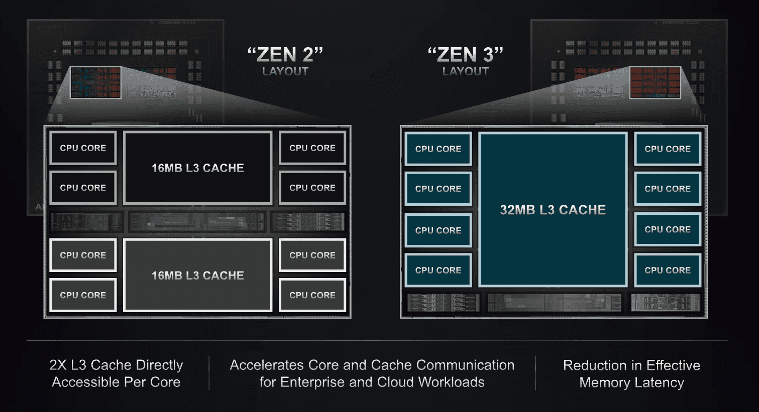
With the Zen 3-based Ryzen 5000 and Milan processors, AMD aims to discard the concept of two CCXs in a CCD. Instead,we’re getting an 8-core CCD (or CCX) with access to the entire 32MB of cache on the die. That means lower core-to-core latency, more cache for each core on the CCD, and wider cache bandwidth. These factors should bring a major performance gain in gaming workloads, as we saw in our review.
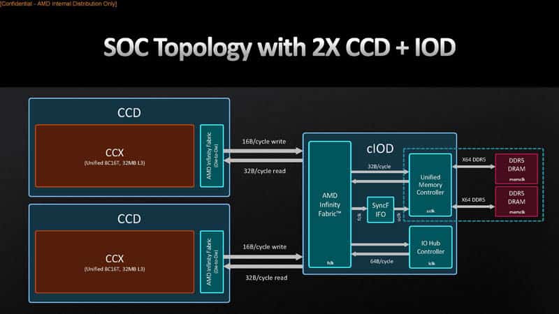
AMD used a bi-directional ring-bus with the Zen 3 CCDs, allowing the transfer of up to 32 bytes of data per cycle, further boosting the bandwidth and reducing latency. The impact is most evident in inter-core bandwidth as we saw in our review.
Team Red uses 16-core CCDs with Zen 4c to design 128-core processors in the form of Bergamo for the cloud market. The mainstream Ryzen and Epyc processors should continue to use the 8-core CCD for the next couple of generations.
Intel’s Monolithic Design and the Future
Keeping the concept of CCDs and CCXs in mind, it’s a lot easier to see the biggest benefit of a chiplet design: scaling. Intel uses what’s called a monolithic approach to CPU design. Every CPU it makes has a discrete design, with a certain number of cores. When manufacturing takes place, all cores in a particular design need to be fully functional. Intel simply throws away partially functional parts. For smaller dual and quad-core processors, this makes a lot of sense: it costs less to manufacture a dual-core processor.

However, since silicon yields are never 100 percent, costs increase exponentially with larger designs. When you get to 10 cores and more, it’s virtually guaranteed that for every functional CPU, Intel discards at least one defective part: keep in mind, only one core needs to be non-functional for the part to be scrapped. In practice, this means that parts in Intel’s Xeon HPC lineup exceed five figures. It also means that there’s an upper limit to the number of cores Intel can viably implement in a single design: Xeon presently tops out at around 40 cores while AMD offers as many as 64 cores with Epyc Rome.

With Sapphire Rapids-SP, Intel is using a chiplet-based (tiled) design with four 20-core dies (two disabled on each). This pushes up the overall core count to 56. The Xeons (Sapphire and Emerald Rapids) were the first blue chips to adopt a chiplet (tiled) design, followed by the consumer-class Core Ultra processors (Meteor Lake) as well.


