Intel’s (formerly 15th Gen) Arrow Lake-S processors are scheduled to launch in the last quarter of 2024. We have known their core counts, architecture, and process nodes. Now, a leak on Chiphell has revealed the I/O capabilities of these processors. Arrow Lake-S will ditch the LGA1700 socket (and the associated 600/700 series motherboards) in favor of LGA1851. The 800-series chipset will be the first to leverage it, including Z890, B860, H870, and H810.
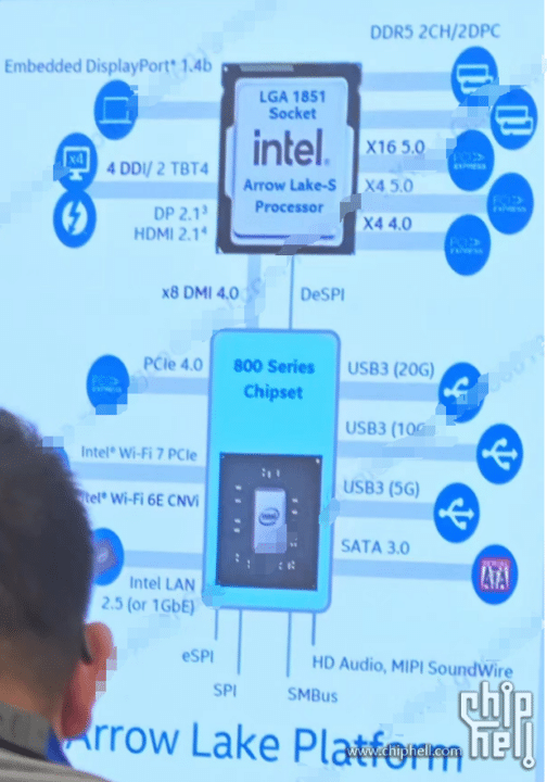
According to the above-leaked image, Intel’s Arrow Lake-S processors will offer 20 PCIe Gen 5 lanes (usable), including 16 for the discrete graphics and four for an M.2 NVMe SSD. There will be another 4-lane PCI Gen 4 cluster for M.2 storage, and x2 Thunderbolt 4 ports (which is new, TBT ports usually come from the IO/chipset).


The same configuration was earlier confirmed in a leak from @yuuki_ans, confirming that the 6P + 8E and 8P + 16E SKUs will feature 20 PCIe Gen 5 lanes. In comparison, AMD’s Ryzen 9000 CPUs will come with 24 PCIe Gen 5 lanes.
Intel, however, has an advantage in the memory department. While AMD’s Ryzen 9000 chips will have a 6000 MT/s or 3000 MHz sweet spot (Infinity fabric in 1:1 ratio), the Arrow Lake chips will have a stock memory frequency of up to 6400 MT/s.
Intel’s 800-series chipsets will feature up to 24 PCIe Gen 4 lanes, 8 SATA III lanes, and 3x GbE ports. The USB ports will comprise 10 USB 3.2 Gen2 x1 (or 5 USB 3.2 Gen 2×2), 14 USB 2, and a BT6/WiFi7 adapter. On the other hand, AMD’s 800-series chipset will feature the following configurations:
| CPU PCIe Lanes | Chipset Lanes | |||||||||
| GRAPHICS | NVMe | USABLE PCIe/PCIe 5.0 | CPU OVERCLOCKING | DDR5 MEMORY OVERCLOCKING/ AMD EXPO | USB 5Gbps | USB 10Gbps | USB 20Gbps | SATA PORTS (OR PCIe 3.0) | USB 4.0 | |
| X870E | 1×16 or 2×8 PCIe 5.0 | 1×4 PCIe 5.0+4x PCIe GPP | 44/24 | Yes | Yes | 2 | 12 | 2 | 8 | STANDARD |
| X870 | 1×16 or 2×8 PCIe 5.0 | 1×4 PCIe 5.0+4x PCIe GPP | 36/24 | Yes | Yes | 1 | 6 | 1 | 4 | STANDARD |
| X670E | 1×16 or 2×8 PCIe 5.0 | 1×4 PCIe 5.0+4x PCIe GPP | 44/24 | Yes | Yes | 2 | 12 | 2 | 8 | optional |
| X670 | 1×16 or 2×8 PCIe 4.0 | 1×4 PCIe 5.0+4x PCIe GPP | 44/8 | Yes | Yes | 2 | 12 | 2 | 8 | optional |
| B650E | 1×16 or 2×8 PCIe 5.0 | 1×4 PCIe 5.0+4x PCIe GPP | 36/24 | Yes | Yes | 1 | 6 | 1 | 4 | optional |
| B650 | 1×16 or 2×8 PCIe 4.0 | 1×4 PCIe 4.0 (or PCIe 5.0) | 36/0 | Yes | Yes | 1 | 6 | 1 | 4 | optional |
| A620/A620A | 1×16 PCIe 4.0 | 1×4 PCIe 4.0 | 32/0 | No | Yes | 2 | 2 | – | 4 | optional |
| PRO 665 | 1×16 or 2×8 | 1×4 PCIe 4.0 (or PCIe 5.0) | 36/0 | No | No | 1 | 6 | 1 | 4 | optional |
| PCIe 4.0 | ||||||||||
| PRO 600 | 1×16 or 2×8 | 1×4 PCIe 4.0+4x PCIe GPP | 28/0 | No | No | 0 | 0 | 0 | 0 | optional |
| PCIe 4.0 | ||||||||||
Via: HXL on X.
Further reading:
Additionally, there has been some speculation regarding the core topography of Arrow Lake. The following design (via 포시포시) is considered fairly accurate:
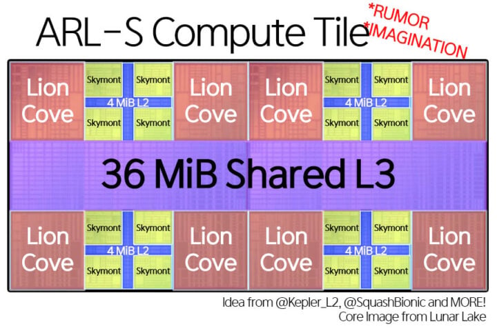
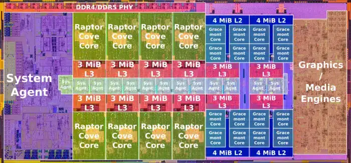
Unlike previous generations, the E-cores have been placed between columns of P-cores. Previously, the P and E-core clusters were separate, like below:
It’s unclear what benefit the newer topography confers, but perhaps it has something to do with inter-core latency or bandwidth.