
AMD is poised to launch the Zen 5 family later this year, including the Ryzen 9000 desktop, mobile, and Epyc server processors. This will be the first time since the introduction of the Zen architecture that all three lineups will land around the same time. The Ryzen 9000 desktop CPUs, codenamed Granite Ridge will likely be revealed at Computex next month.
The mobile stack consisting of Strix Point and Strix Halo should follow shortly after in the fall. The Epyc Turin server chips will likely target a Q4 release, with the Zen 5c-based “Dense” SKUs meant for the cloud market preceding Turin “Classic” or Zen 5.

AMD Ryzen 9000 “Granite Ridge” AM5 Desktop CPUs Specs and Release
AMD will likely unveil the Ryzen 9000 “Granite Ridge” processors for the AM5 desktop platform at Computex 2024. Company CEO Dr. Lisa Su confirmed this during AMD’s past earnings call. The chipmaker’s official roadmap aligns with this launch window.
Looking back at AMD’s previous launches, the Ryzen 5000 CPUs were launched in October 2020, while the Ryzen 7000 series landed in September 2022. Both lineups were announced at the preceding Computex events, followed by a retail launch in the fall. The Ryzen 9000 processors should follow the trend with a Q3 2024 release. According to rumors, the Zen 5 chips are already in mass production.
| Ryzen 9 9950X | Ryzen 7 9700X | |
|---|---|---|
| Cores/Threads | 16/32 | 8/16 |
| L2 Cache (per core) | 1MB | 1MB |
| L3 Cache (shared) | 64MB | 32MB |
| Boost Clock | 6GHz? | 6GHz? |
| PCIe Lanes (Gen 5) | 24? | 24? |
| Memory Support | DDR5-6000? | DDR5-6000? |
| TDP | 170W | 170W |
| PPT | 230W | 230W |
| Process | TSMC 4nm | TSMC 4nm |
| Launch | Q3 2024 | Q3 2024 |
The Ryzen 9000 desktop lineup will feature up to 16 cores (32 threads) spread across two 8-core CCDs, each packing 32MB of unified L3 cache, and 64MB total. The Zen 5 dies will be fabbed on TSMC’s 4nm process, while the I/O will be 6nm.
AMD Zen 5 Strix Point, Strix Halo, and Kraken Point Mobile CPUs: Specs and Release

The Ryzen 9000 mobile family will be massive, consisting of Strix Point, Strix Halo, Kraken Point, Sonoma Valley, and Fire Range. These chips will feature an upgraded CPU, GPU, and NPU. The Zen 5 cores will be paired with the Zen 5c “E-cores,” marking the release of AMD’s first true hybrid core processors.
We will also take the next major step in our AI PC road map later this year with the launch of our next-generation Ryzen mobile processors code named Strix. Customer interest in Strix is very high based on the significant performance and energy efficiency uplifts we are delivering. Design win momentum for premium notebooks is outpacing prior generations as Strix enables next-generation AI experiences in laptops that are thinner, lighter and faster than ever before. We’re excited about the growth opportunities for the PC market. And based on the strength of our Ryzen CPU portfolio, we expect to grow revenue share this year.
Dr. Lisa Su, AMD CEO
The RDNA 3+ graphics architecture will debut, offering dGPU-level gaming performance at a much lower power budget. Strix Point will also feature a next-gen NPU based on the XDNA 2 architecture, offering 2-3x the inferencing throughput as Hawk Point.
- 45-75W->
- Strix Halo (chiplet-based): 16x Zen 5 on TSMC N4P: FP11.
- GPU: 40x RDNA 3.5 CUs.
- L2 Cache: 16MB (1MB per core).
- L3 Cache: 64MB (shared).
- NPU: 75T?
- Strix Halo (chiplet-based): 16x Zen 5 on TSMC N4P: FP11.
- 15-54W->
- Strix Point (hybrid, monolithic U/H): 4x Zen 5 + 8x Zen 5c on TSMC N4P: FP8.
- GPU: 16x RDNA 3.5 CUs @ 2.6-2.7GHz.
- L2 Cache: 12MB (1MB per core).
- L3 Cache: 24 MB (16MB + 8MB).
- NPU: 45T?
- Kraken Point (hybrid, monolithic U/H): 4x Zen 5 + 4x Zen 5c on TSMC N4P: FP8.
- GPU: 8x RDNA 3.5 CUs.
- NPU: 45T?
- Strix Point (hybrid, monolithic U/H): 4x Zen 5 + 8x Zen 5c on TSMC N4P: FP8.
- 9-15W->
- Sonoma Valley (monolithic U): 8x Zen 5c on Samsung SF4P: FP6.
- GPU: 2x RDNA 3.5.
- NPU: N/A.
- Sonoma Valley (monolithic U): 8x Zen 5c on Samsung SF4P: FP6.

The Ryzen 9000 mobile family will comprise the following lineups:
- Strix Point: These CPUs will likely form the Ryzen 9040 series, combining Zen 5 and Zen 5c cores in a monolithic design on the FP8 package. Expect up to 12 cores, including 4x Zen 5 and 8x Zen 5c working in tandem.
- The iGPU will feature (up to) 16x RDNA 3.5 Compute Units and a 60+ TOP NPU unit. Strix will power ultrathin (U) and performance (H) notebooks in the 15-54W segments.
- Strix Halo: Strix Halo will allegedly feature a chiplet design packing up to 16 Zen 5 cores (8C x2) and a beastly iGPU with 40 Compute Units (RDNA 3.5). Like Strix Point, it’ll also feature a powerful NPU for AI workloads packaged on FP11. The TDP range will vary from 45W to 75W, targeting gaming and content creation notebooks (H).
- Fire Range: This is a bit murky. Fire Range is supposed to be the successor to Dragon Range featuring repurposed AM5 “Granite Ridge” CPUs with reduced clocks and power limits. These will form the Ryzen 9045HX series, consisting of a 3D V-Cache part similar to the R9 7945HX3D.
- Kraken Point: Kraken Point will resemble Strix Point, but reduce the core counts and TDPs, making it suitable for ultrabooks and convertibles. It will likely have a TDP range of 15-28W (U/H) and utilize the FP8 package.
- Sonoma Valley: Sonoma Valley is an oddity and will likely be used for Chromebooks. It allegedly features only Zen 5c cores (up to 8) on the FP6 package and will be fabbed on Samsung’s 4nm node. It will have a TDP of 9-15W with a pair of RDNA 3 Compute Units, but no NPU.
AMD Epyc Turin Specs and Release Date
The Epyc Turin family will be much more diverse than Genoa consisting of Turin Dense, Turin-X, Turin Classic, Turin AI, and Sorano (succeeding Siena). Turin Classic will offer up to 128 Zen 5 cores for traditional server and data center clients while Turin Dense will serve the Cloud market with core counts of up to 160 (Zen 5c).

Like Genoa, Turin will retain the SP5 (LGA-6096) socket. The TDP of the “Classic” Zen 5 CPUs will vary from 200W on the lower-end SKUs to 400W on the flagship models. The L3 cache is unchanged at 32MB per CCD, implying a total Last Level Cache (LLC) of 384MB and 512MB for 96-core and 128-core variants, respectively.
Looking ahead, we’re very excited about our next-gen Turin family of EPYC processors featuring our Gen 5 core. We’re widely sampling Turin, and the silicon is looking great. In the cloud, the significant performance and efficiency increases of Turin position us well to capture an even larger share of both first and third-party workloads. In addition, there are 30% more Turin platforms in development from our server partners, compared to fourth-gen EPYC platforms, increasing our enterprise and with new solutions optimized for additional workloads. Turin remains on track to launch later this year.
Dr. Lisa Su, AMD CEO
The Epyc Turin “Dense” Zen 5c lineup will feature up to 160 cores and 320 threads. These are clocked at just over 2GHz for the “denser” flagship SKUs with an L3 cache of up to 320MB (32MB per 16-core CCD). As per rumors, there will be only three Turin Dense chips with TDPs of up to 500W. Turin Classic “Zen 5” and Dense “Zen 5c” are slated to land later this year.

Turin-X is expected in early 2025 with 1.536GB of L3 cache (3D V-Cache) and roughly the same core counts as Turin Classic. Turin AI should launch simultaneously with Zen 5c cores and an AI chiplet featuring a neural accelerator. Then there’s Sorano, a budget and power-efficient variant of Turin Dense with up to 64 cores and a TDP of 225W.
The Zen 5 Core Architecture
Zen 5 Front End
The Zen 5 core architecture (codenamed Nirvana) will be a major upgrade over Zen 4, with a reworked frontend and a wider backend. Starting from the top, the L1D cache has been increased from 32KB to 48KB (12-way), complemented by an expanded Data Translation Buffer and a recalibrated branch predictor.
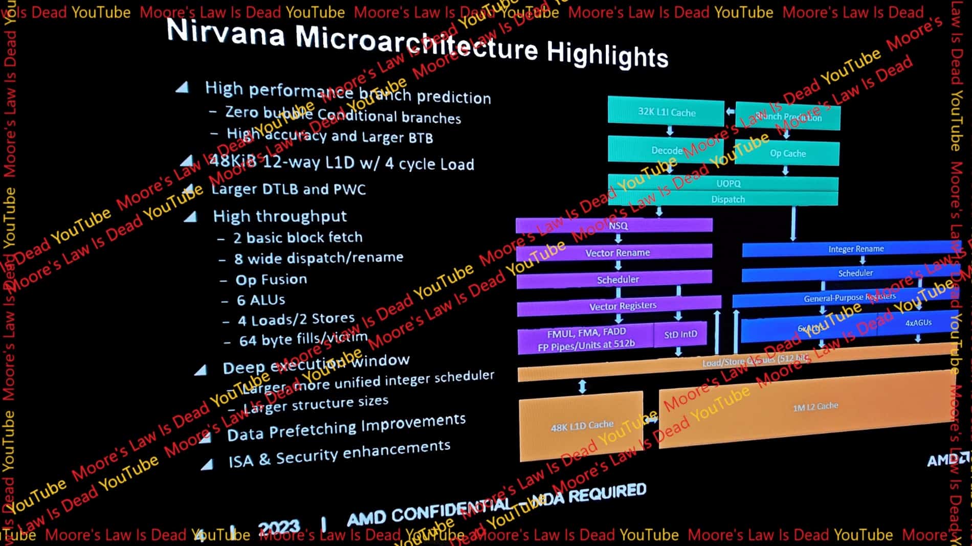
In out-of-order CPUs, the branch predictor is one of the most important components. Sitting at the top of the pipeline, it controls the instruction flow along with the Branch Target Buffer (BTB), which has also been upgraded. Zen 5’s branch predictor executes “Zero bubble” conditional branches. This implies that conditional branches are taken without interrupting or stalling the pipeline.
The decoder looks unchanged (4-way) with a 2-basic block fetch. The rename/dispatch buffer has been consolidated to simultaneously process up to 8 micro-ops (previously 6) with support for op-fusion. This allows two micro-ops from the same instruction to be treated as one at some points in the pipeline, doubling the effective throughput.
The Dispatch will also be upgraded from 6 maco-ops on Zen 4 to 8 macro-ops on Zen 5, keeping the backend fed at all times.
Zen 5 Backend

Zen 5 strengthens AMD’s already formidable Integer Execution. The integer scheduler has been reinforced into a unified queue with “larger structure sizes.” This means that multiple smaller scheduler windows have been consolidated into larger queues (4->2). The integer ALU count has been increased to 6 (previously 4) to accommodate the higher throughput.
A fourth AGU (Address Generation Unit) has also been added to keep the load-store queues fed. Overall, we’ve got 10 execution ports on Zen 5’s Integer backend. The Load/Store bandwidth has been expanded to 4 loads (previously 3) or two stores per cycle.

On the Floating Point end, all four execution ports have been doubled in width to 512-bit to support AVX-512 instructions. A fifth port consisting of two 256-bit units has also been added. The expanded EUs mean larger floating point registers to sustain them, substantially larger. For comparison, Intel designs only consist of one or two 512-bit units per core.
Ladder L3 Fabric and Infinity Fabric Gen 3
AMD’s Ryzen 8000 processors will use an upgraded core interconnect known as the Ladder L3 Fabric (originally leaked by AdoredTV). This is related to the 3rd Gen Infinity Fabric, which will act as the die interconnects for AMD’s next generation of chiplet products. This bus impacts the core-to-core latency and bandwidth, which is crucial in gaming workloads. MLID claims that the fabric will be clocked at 2400MHz with a memory target of DDR5-8000 using EXPO.

AM5 800 Series Motherboards
AMD is working on an 800-series chipset for Zen 5 that will launch ahead of the Ryzen 9000 processors. The flagship X870E chipset will feature two Promontory 21 chips and an ASM4242 USB 4 controller. The inclusion of up to 20 PCIe 5 lanes (for dGPU and NVMe) will be the highlight. The B850 chipset will be the core of AMD’s next-gen budget offerings. It will sport PCIe Gen 5 support for at least the dGPU slot (x8 or x16?).
A B840 chipset based on Promontory 19 is also planned, but details remain sparse. AMD has set a memory target of DDR5-8000 for the Ryzen 9000 CPUs (with EXPO profiles), with an Fclk target of 2400MHz. The latter shouldn’t be an issue as the Ryzen 8000G processors are already designed for fabric clocks of 2400MHz and higher.
AMD Ryzen 9000X3D and Zen 5 V-Cache
According to Kepler, the Ryzen 9000X3D processors (Zen 5 3D V-Cache) will be revealed during CES 2025, slated to be held in the first week of January 2025. If the Ryzen 9000 “Zen 5” CPUs launch between summer and fall (June to September), then a 6-month gap separating them from the 3D V-Cache variants makes sense. This will depend on when Intel launches its 15th Gen Arrow Lake processors. They’ll have a similar effect on the market as Raptor Lake.
Frequently Asked Questions
- Will the Ryzen 9000 CPUs be compatible with existing AM5 motherboards (A620/B650/B650E/X670/X670E)?
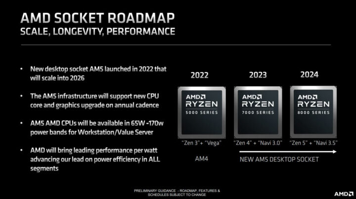
AMD has officially confirmed that the AM5 socket will be supported through 2025. At the very least, the existing 600-series motherboards will be fully compatible with the Ryzen 9000 CPUs. Some board partners have already released firmware enabling support for the next-gen Zen 5 processors.
- When will the Ryzen 9000 CPUs be available for purchase?
There’s no official confirmation, but we expect the next-gen processors to hit retail sometime in September 2024.
- How fast will the Ryzen 9000 CPUs be compared to the 7000 series and Intel’s Raptor Lake offering?
The Zen 5 core architecture is shaping up to be an impressive feat of engineering. According to leaked benchmarks and rumors, the Ryzen 9000 chips will be 30-40% faster than their Ryzen 7000 predecessors. Some even claim an uplift of 60-80%, but I’d take them with a grain of salt.


